- 您现在的位置:买卖IC网 > Sheet目录3881 > PIC18F8585T-I/PT (Microchip Technology)IC PIC MCU FLASH 24KX16 80TQFP
PIC18F6585/8585/6680/8680
DS30491C-page 168
2004 Microchip Technology Inc.
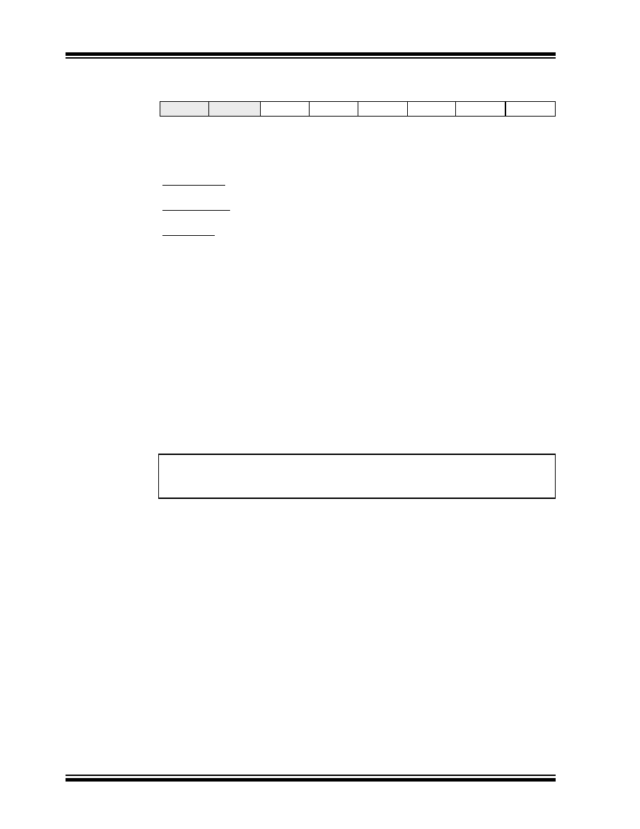
REGISTER 15-2:
CCP2CON REGISTER
U-0
R/W-0
—
DC2B1
DC2B0
CCP2M3
CCP2M2
CCP2M1
CCP2M0
bit 7
bit 0
bit 7-6
Unimplemented: Read as ‘0’
bit 5-4
DC2B1:DC2B0: PWM Duty Cycle bit 1 and bit 0
Capture mode:
Unused.
Compare mode:
Unused.
PWM mode:
These bits are the two LSbs of the 10-bit PWM duty cycle. The eight MSbs of the duty cycle are
found in CCPR2L.
bit 3-0
CCP2M3:CCP2M0: CCP2 Mode Select bits
0000
= Capture/Compare/PWM off (resets CCP2 module)
0001
= Reserved
0010
= Compare mode, toggle output on match
0011
= Reserved
0100
= Capture mode, every falling edge
0101
= Capture mode, every rising edge
0110
= Capture mode, every 4th rising edge
0111
= Capture mode, every 16th rising edge
1000
= Compare mode, initialize CCP pin low, on compare match force CCP pin high
1001
= Compare mode, initialize CCP pin high, on compare match force CCP pin low
1010
= Compare mode, generate software interrupt only, CCP pin is unaffected
1011
= Compare mode, trigger special event, resets TMR1 or TMR3 and starts A/D conversion
if A/D module is enabled
11xx
= PWM mode
Legend:
R = Readable bit
W = Writable bit
U = Unimplemented bit, read as ‘0’
- n = Value at POR
‘1’ = Bit is set
‘0’ = Bit is cleared
x = Bit is unknown
发布紧急采购,3分钟左右您将得到回复。
相关PDF资料
XF2J-2424-11
CONN FPC 24POS 0.5MM SMT
PIC18LF6585T-I/PT
IC PIC MCU FLASH 24KX16 64TQFP
PIC18LF6680T-I/PT
IC PIC MCU FLASH 32KX16 64TQFP
XF2J-2224-11
CONN FPC 22POS 0.5MM SMT
PIC18F6525T-I/PT
IC PIC MCU FLASH 24KX16 64TQFP
PIC18F4439-E/ML
IC PIC MCU FLASH 6KX16 44QFN
XF2J-2024-11
CONN FPC 20POS 0.5MM SMT
PIC16LF747-I/ML
IC PIC MCU FLASH 4KX14 44QFN
相关代理商/技术参数
PIC18F85J10-I/PT
功能描述:8位微控制器 -MCU 32 KB FL 2 KB RAM RoHS:否 制造商:Silicon Labs 核心:8051 处理器系列:C8051F39x 数据总线宽度:8 bit 最大时钟频率:50 MHz 程序存储器大小:16 KB 数据 RAM 大小:1 KB 片上 ADC:Yes 工作电源电压:1.8 V to 3.6 V 工作温度范围:- 40 C to + 105 C 封装 / 箱体:QFN-20 安装风格:SMD/SMT
PIC18F85J10-I/PT
制造商:Microchip Technology Inc 功能描述:IC 8BIT MCU PIC18F 40MHZ TQFP-80 制造商:Microchip Technology Inc 功能描述:IC, 8BIT MCU, PIC18F, 40MHZ, TQFP-80
PIC18F85J10T-I/PT
功能描述:8位微控制器 -MCU 32 KB FL 2 KB RAM RoHS:否 制造商:Silicon Labs 核心:8051 处理器系列:C8051F39x 数据总线宽度:8 bit 最大时钟频率:50 MHz 程序存储器大小:16 KB 数据 RAM 大小:1 KB 片上 ADC:Yes 工作电源电压:1.8 V to 3.6 V 工作温度范围:- 40 C to + 105 C 封装 / 箱体:QFN-20 安装风格:SMD/SMT
PIC18F85J11-I/PT
功能描述:8位微控制器 -MCU 32KB Flash 2048BRAM 67I/O RoHS:否 制造商:Silicon Labs 核心:8051 处理器系列:C8051F39x 数据总线宽度:8 bit 最大时钟频率:50 MHz 程序存储器大小:16 KB 数据 RAM 大小:1 KB 片上 ADC:Yes 工作电源电压:1.8 V to 3.6 V 工作温度范围:- 40 C to + 105 C 封装 / 箱体:QFN-20 安装风格:SMD/SMT
PIC18F85J11T-I/PT
功能描述:8位微控制器 -MCU 32KB Flash 2048bytes-RAM 67I/O RoHS:否 制造商:Silicon Labs 核心:8051 处理器系列:C8051F39x 数据总线宽度:8 bit 最大时钟频率:50 MHz 程序存储器大小:16 KB 数据 RAM 大小:1 KB 片上 ADC:Yes 工作电源电压:1.8 V to 3.6 V 工作温度范围:- 40 C to + 105 C 封装 / 箱体:QFN-20 安装风格:SMD/SMT
PIC18F85J15-I/PT
功能描述:8位微控制器 -MCU 48 KB FL 4 KB RAM RoHS:否 制造商:Silicon Labs 核心:8051 处理器系列:C8051F39x 数据总线宽度:8 bit 最大时钟频率:50 MHz 程序存储器大小:16 KB 数据 RAM 大小:1 KB 片上 ADC:Yes 工作电源电压:1.8 V to 3.6 V 工作温度范围:- 40 C to + 105 C 封装 / 箱体:QFN-20 安装风格:SMD/SMT
PIC18F85J15T-I/PT
功能描述:8位微控制器 -MCU 48 KB FL 4 KB RAM RoHS:否 制造商:Silicon Labs 核心:8051 处理器系列:C8051F39x 数据总线宽度:8 bit 最大时钟频率:50 MHz 程序存储器大小:16 KB 数据 RAM 大小:1 KB 片上 ADC:Yes 工作电源电压:1.8 V to 3.6 V 工作温度范围:- 40 C to + 105 C 封装 / 箱体:QFN-20 安装风格:SMD/SMT
PIC18F85J50-I/PT
功能描述:8位微控制器 -MCU 32KB Flash 3936byte RAM RoHS:否 制造商:Silicon Labs 核心:8051 处理器系列:C8051F39x 数据总线宽度:8 bit 最大时钟频率:50 MHz 程序存储器大小:16 KB 数据 RAM 大小:1 KB 片上 ADC:Yes 工作电源电压:1.8 V to 3.6 V 工作温度范围:- 40 C to + 105 C 封装 / 箱体:QFN-20 安装风格:SMD/SMT